Photovoltaics: Clean Electricity for the 21st Century
By Alvin Compaan
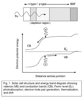
 Fig. 1 indicates the typical construction of the semiconductor part of a Si cell. |
Microprocessors, semiconductor memories, light-emitting diodes and other solid-state electronics typically have high commercial value and small sizes ranging from a few square microns to a few square centimeters. Thus they can be made in large quantities and often can be individually tested before being incorporated into the consumer product. Although early photovoltaic (PV) cells and modules were used in space and other off-grid applications where their value is high, currently about 70% of PV is grid- connected which imposes major cost pressures from conventional sources of electricity. Yet the potential benefits of its large-scale use are enormous and PV now appears to be meeting the challenge with annual growth rates above 30% for the past five years.
More than 90% of PV is currently made of Si modules assembled from small 4-12 inch crystalline or multicrystalline wafers which, like most electronics, can be individually tested before assembly into modules. However, the newer thin-film technologies are monolithically integrated devices approximately 1 m2 in size which cannot have even occasional shunts or weak diodes without ruining the manufacturing yield. Thus, these devices require the deposition of many thin semiconducting layers on glass, stainless steel or polymer and all layers must function well a square meter at a time or the device fails. This is the challenge of PV technology-high efficiency, high uniformity, and high yield over large areas to form devices that can operate with repeated temperature cycles from —40 C to 100 C with a provable twenty- year lifetime and a cost of less than a penny per square centimeter.
Solar cells work and they last. The first cell made at Bell Labs in 1954 is still functioning. Solar cells continue to play a major role in the success of space exploration—witness the Mars rovers. Today's commercial solar panels, whether of crystalline Si, thin amorphous, or polycrystalline films, are typically guaranteed for 20 years—unheard of reliability for a consumer product. However, PV still accounts for less than 10-5 of total energy usage world-wide. In the US, electricity produced by PV costs upwards of $0.25/ kW-hr whereas the cost of electricity production by coal is less than $0.04 /kW-hr.
It seems fair to ask what limits the performance of solar modules and is there hope of ever reaching cost- competitive generation of PV electricity?
The photogeneration of a tiny amount of current was first observed by Adams and Day in 1877 in selenium. However, it was not until 1954 that Chapin, Fuller and Pearson at Bell Labs obtained significant power generation from a Si cell. Their first cells used a thick lithium-doped n-layer on p-Si, but efficiencies rose well above 5% with a very thin phosphorous-doped n-Si layer at the top.
The traditional Si solar cell is a homojunction device. The sketch of Fig. 1 indicates the typical construction of the semiconductor part of a Si cell. It might have a p-type base with an acceptor (typically boron or aluminum) doping level of NA = 1 x 1015 cm-3 and a diffused n-type window/emitter layer with ND = 1 x 1020 cm-3 (typically phosphorus). The Fermi level of the n-type (p-type) side will be near the conduction (valence) band edge so that donor-released electrons will diffuse into the p-type side to occupy lower energy states there, until the exposed space charge (ionized donors in the n-type region, and ionized acceptors in the p-type) produces a field large enough to prevent further diffusion. Often a very heavily doped region is used at the back contact to produce a back surface field (BSF) that aids in hole collection and rejects electrons.
In the ideal case of constant doping densities in the two regions, the depletion width, W, is readily calculated from the Poisson equation, and lies mostly in the lightly doped p-type region. The electric field has its maximum at the metallurgical interface between the n- and p-type regions and typically reaches 104 V/cm or more. Such fields are extremely effective at separating the photogenerated electron-hole pairs. Silicon with its indirect gap has relatively weak light absorption requiring about 10-20μm of material to absorb most of the above-band-gap, near-infrared and red light. (Direct-gap materials such as GaAs, CdTe, Cu(InGa)Se2 and even a-Si:H need only ~0.5μm or less for full optical absorption.) The weak absorption in crystalline Si means that a significant fraction of the above-band-gap photons will generate carriers in the neutral region where the minority carrier lifetime must be very long to allow for long diffusion lengths. By contrast, carrier generation in the direct-gap semiconductors can be entirely in the depletion region where collection is through field-assisted drift.
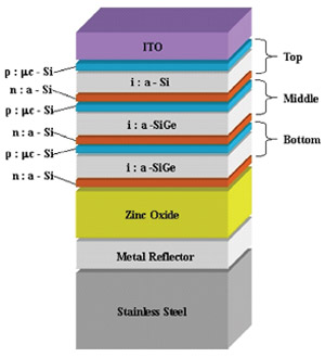
 Fig. 2. Triple junction a-Si/a-SiGe/a-SiGe cell structure (courtesy X. Deng/U. Toledo) |
A high quality Si cell might have a hole lifetime in the heavily doped n-type region of tp=1μs and corresponding diffusion length of Lp=12 μm, whereas, in the more lightly doped p-type region the minority carriers might have tn=350 μs and Ln=1100 μm. Often few carriers are collected from the heavily doped, n-type region so strongly-absorbed blue light does not generate much photocurrent. Usually the n-type emitter layer is therefore kept very thin. The long diffusion length of electrons in the p- type region is a consequence of the long electron lifetime due to low doping and of the higher mobility of electrons compared with holes. This is typical of most semiconductors so that the most common solar cell configuration is an "n-on-p" with the p-type semiconductor serving as the "absorber."
Current generated by an ideal, single-junction solar cell is the integral of the solar spectrum above the semiconductor band gap and the voltage is approximately 2/3 of the band gap. Note that any excess photon energy above the band edge will be lost as the kinetic energy of the electron and hole pair relaxes to thermal motion in picoseconds and simply heats the cell. Thus single-junction solar cell efficiency is limited to about 30% for band gaps near 1.5 eV. Si cells have reached 24%.
This limit can be exceeded by multijunction devices since the high photon energies are absorbed in wider-band-gap component cells. In fact the III-V materials, benefiting like Si from research for electronics have been very successful at achieving very high efficiency, reaching 35% with the monolithically stacked three-junction, two-terminal structure, GaInP/GaAs/Ge. These tandem devices must be critically engineered to have exactly matched current generation in each of the junctions and therefore are sensitive to changes in the solar spectrum during the day. A sketch of a triple-junction, two-terminal amorphous silicon cell is shown in Fig. 2.
Polycrystalline and amorphous thin-film cells use inexpensive glass, metal foil or polymer substrates to reduce cost. The polycrystalline thin film structures utilize direct-gap semiconductors for high absorption while amorphous Si capitalizes on the disorder to enhance absorption and hydrogen to passivate dangling bonds. It is quite amazing that these very defective thin-film materials can still yield high carrier collection efficiencies. Partly this comes from the field-assisted collection and partly from clever passivation of defects and manipulation of grain boundaries. In some cases we are just lucky that nature provides benign or even helpful grain boundaries in materials such as CdTe and Cu(InGa)Se2, although we seem not so fortunate with GaAs grain boundaries. It is now commonly accepted that, not only are grain boundaries effectively passivated during the thin-film growth process or by post-growth treatments, but also that grain boundaries can actually serve as collection channels for carriers. In fact it is not uncommon to find that the polycrystalline thin-film devices outperform their single-crystal counterpart.
In the past two decades there has been remarkable progress in the performance of small, laboratory cells. The common Si device has benefited from light trapping techniques, back-surface fields, and innovative contact designs, III-V multijunctions from high quality epitaxial techniques, a-Si:H from thin, multiple-junction designs that minimize the effects of dangling bonds (Stabler-Wronski effect), and polycrystalline thin films from innovations in low-cost growth methods and post-growth treatments. These laboratory successes are now being translated into success in the manufacturing of large PV panel sizes in large quantities and with high yield. The worldwide PV market has been growing at 30% to 40% annually for the past five years due partly to market incentives in Japan and Germany, and more recently in some U.S. states.
Recent analyses of the energy payback time for solar systems show that today's systems pay back the energy used in manufacturing in about 3.5 years for silicon and 2.5 years for thin films.
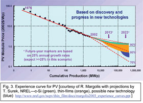
 Fig 3. The decline of manufacturing costs follows nicely an 80% experience curve-costs dropping 20% for each doubling of cumulative production. |
The decline of manufacturing costs follows nicely an 80% experience curve-costs dropping 20% for each doubling of cumulative production. (See Fig. 3.) The newly updated PV Roadmap (http://www.seia.org) envisions PV electricity costing $0.06/kW-hr by 2015 and half of new U.S. electricity generation to be produced by PV by 2025, if some modest and temporary nationwide incentives are enacted. Given the rate of progress in the laboratory and innovations on the production line, this ambitious goal might just be achievable. PV can then begin to play a significant role in reducing greenhouse gas emissions and in improving energy security. Some analysts see PV as the only energy resource that has the potential to supply enough clean power for a sustainable energy future for the world.
Alvin Compaan is Professor of Physics and Department Chair, and Director of the Center for Materials Science and Engineering at the Department of Physics and Astronomy, the University of Toledo.
©1995 - 2024, AMERICAN PHYSICAL SOCIETY
APS encourages the redistribution of the materials included in this newspaper provided that attribution to the source is noted and the materials are not truncated or changed.
Associate Editor: Jennifer Ouellette
April 2005 (Volume 14, Number 4)
Articles in this Issue

