Time-Resolved Emission Microscopy of Silicon Integrated Circuits
By Stanislav Polonsky
Background
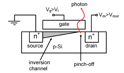
When asked about the light emission in semiconductors we tend to think about devices such as light emitting diodes or semiconductor lasers. It is less known that the silicon metal-oxide-semiconductor field-effect transistor (MOSFET), a workhorse of modern integrated circuits (IC) technology, can also emit light. The emission takes place when a MOSFET is in saturation (see Fig. 1). In saturation, the current through the device practically does not depend on drain voltage since the conducting channel is pinched off. The voltage drop across this pinched -off region gives rise to high electric field (>105 V/cm). The Light Emission in Saturation (LSAT) arises from the relaxation of hot electrons created by this field. Its broad spectrum covers visible and near infrared regions. For the majority of people the idea of using a MOSFET as a light source may seem strange and useless. Still, it finds important applications in the area of semiconductor IC testing and debug, known as photon emission microscopy (PEM) of IC.
 Fig.1. Light emission from saturated n-type MOSFET |
In the dominant Complementary Metal-Oxide-Semiconductor (CMOS) technology, the voltage drop across a conducting transistor is close to zero, so a MOSFET can never be permanently in saturation, provided that a circuit works properly and it is in a well defined logic state. In a circuit with a fault such as a shorted or open wire, the MOSFET can stay in saturation, and the light emission from it can assist in localizing the fault. This fact explains the power of PEM in IC defect localization. For completeness, it is worth mentioning that PEM also uses another light emission mechanism–radiative electron-hole recombination. In bulk CMOS technologies it can occur when two parasitic bipolar transistors latch up.
When a properly working CMOS circuit switches, some of its MOSFETs can be driven into saturation for a short period of time. The resulting LSAT is very weak–it produces less than a photon per transistor per switch; detecting LSAT requires single photon detectors. The transient emission from a CMOS circuit was first detected by two IBM researchers, Jeffrey Kash and James Tsang, in 1996. Using a thermoelectrically cooled microchannel plate (MCP) photomultiplier with a position sensitive resistive anode, they detected short (<270 ps) pulses from a fully functional ring oscillator fabricated in 0.6 mm CMOS technology running at voltage VDD=3.5V. Analysis of arrival times of such pulses and correlating them with particular transistors allows one to reconstruct the switching dynamics of a circuit and provides invaluable information about its internal operation. The invented technique became known as PICA– Picosecond Imaging Circuit Analysis.
Applications
PICA enjoyed a lucky history–immediate industrial applications followed soon. In late 1997 an IBM team measured the clock tree skew in 0.25 mm 64-bit 2.5V CMOS microprocessor running at 100 MHz. The measurements were performed from a thinned and polished back side of the chip.
PICA was first licensed by the Schlumberger Probe System Group. At present, an Emiscope® product line, capable of performing time-resolved emission microscopy, is available from Credence Systems corporation. As a result of increased availability of commercial tools, PICA has become a standard technique in failure analysis labs of many semiconductor corporations.
Challenges of CMOS scaling
CMOS scaling is presenting a number of challenges to maintaining the usefulness of PICA: low voltage operation, high power chips, and shorter channel lengths of transistors.
Lowering power supply voltage VDD is a necessary consequence of CMOS scaling. Since the invention of PICA, it dropped from 3.5 V down to 1V. This has drastically influenced the choice of single photon time-resolved detectors for PICA. Decreasing power supply voltage shifts emission spectra into longer wavelengths and exponentially decreases its intensity. The MCP imaging detectors with S-25 photocathod are sensitive in 400-900 nm range. For backside measurements, which is the only viable option for modern flip-chip packaged microprocessors, most of the emission in this spectral range is blocked by silicon. MCP continued to be useful as technology approached VDD=1.8 V (180 nm technology node). For 180 nm chips running at nominal voltage typical acquisition time could easily be as long as tens of hours. For next generations, a new type of the detector was needed, developed by the group of physicists from Moscow State Pedagogical University (MSPU), led by Professor Gregory Goltsman, and in collaboration with Rochester University. Named Superconduct-ing Single Photon Detector (SSPD), the detector operates by producing short voltage pulses when a single photon is absorbed in a sub-critically current-biased superconducting nano-wire. It had quantum detection efficiency QE=5% at wavelength 1.3 m and timing jitter (i.e. photon detection time error) about 40 ps. The detector operates at temperature T=2÷3 K. SSPD-based tools are thousands times faster than those based on MCT, and they demonstrate short measurement times (minutes) when debugging modern 90 nm microprocessors running at VDD≈1V. Our experience shows they will also be adequate for coming 65 nm microprocessors. The price paid for achieving such performance was abandoning imaging capabilities of the original technique and using single pixel detectors.
An alternative approach was chosen by researchers from Credence Systems Corporation. They used a thermoelectrically cooled InGaAs avalanche photodiode with custom quenching electronics as a single photon detector. At expense of higher dark count, it achieves impressive QE>10%.
Increasing power dissipation, which could be more than 100 W in modern microprocessor, is also a growing concern. Indeed, backside PICA measurements require removal of a heat sink, without which the chip just does not work properly. Blowing dry nitrogen on a chip can sometimes alleviate the problem, especially for relatively simple application-specific integrated circuits (ASICs). The permanent solution is diamond heat spreaders, or even water cooling.
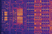
 Fig. 2. Off-state emission from a quiescent 130 nm microprocessor. Brighter colors correspond to more intense emission. |
Shorter transistor channel length Lch is also a consequence of CMOS scaling. Denser placement of transistors makes it difficult to resolve them optically. Resolution of Si subsurface imaging is limited to 0.5 mm. Solid immersion lenses (SIL) can improve diffraction-limited resolution and light collection efficiency by an order of magnitude. They are becoming a standard feature of PEM tool manufactures.
Another consequence of decreasing Lch is increasing off-state drain-to-source leakage c urrent and electric field in the channel. Taken together, these two factors give rise to hot electron populations sufficient to emit a measurable amount of light even when the device is in off-state. Such off-state light emission (LOFF) becomes noticeable in devices from 180 nm technology generation and dramatically increases for subsequent generations (see Fig. 2). While being a consequence of a highly undesirable effect, leakage currents in MOSFETs, LOFF can be put to use in IC emission microscopy. Fig. 3 illustrates the concept of off-state light emission from a CMOS inverter. N-type MOSFET emits off-state light LN only when the inverter is in logic state 1 while p-type MOSFET emits light LP only when the inverter is in logic state 0. The leakage emission from both types of devices is persistent–the devices emit the light as long as the inverter is in a definite state. For practical purposes, it is possible to say that LOFF tracks leakage current with one important advantage–it can be easily measured using standard tools of photon emission microscopy. Off-state leakage current and, consequently, LOFF depend on a number of parameters that are difficult to measure on a chip: internal voltages, device temperature, channel length, threshold voltage, etc. The ability to non-invasively measure these parameters is important for IC design and fabrication. For example, knowing the on-chip voltage variations caused by wire crosstalk noise, inductive interconnect response, and power grid noise caused by circuit switching activity are crucial for signal integrity characterization of modern high speed digital IC.
 Fig. 3. Light emission from n-type MOSFET (LN) and p-type MOSFET (LP) in a CMOS inverter is a combination of LSAT and LOFF: LOFF (horizontal region) “tracks” the logic state of a transistor; LSAT (peaks) corresponds to the emission from switching transistors. Light emission from n-type devices is much stronger than that from p-type devices. |
Time-resolved measurements of off-state emission allowed our group to extract optically the dynamics of gate and drain voltages across a single MOSFET with accuracy few mV. We were also able measure the dynamics of Silicon-on-Oxide MOSFET self-heating, using the dependence of off-state emission on device temperature. The dependence of off-state emission on the logic state of a circuit can be used to localize a resistive fault in a microprocessor. One of the most recent developments is optical characterization of across chip device performance variations which become more and more important as transistor size shrinks and it becomes more difficult to control its parameters. Smaller Lch and Vt make MOSFET to switch faster, and, simultaneously, increase LOFF. We used this fact to optically map device performance variations within a single chip.
Opportunities
Measurements of transistor switching times will probably continue to be the major application of PICA. Our experience with next generation technologies, which are presently being under development, indicates that the light emission from the future MOSFETs is strong enough to be measured by existing single photon detectors. The major opportunities lie in the PICA tools area. Making the analysis easy to use, integrating it with other failure analysis techniques (e.g. thermal imaging) will determine further adoption of PICA by the industry.
There are opportunities in adding value to PICA by utilizing new sources of light emission such as off-state current, or using time-resolved spectroscopic data. Also, in recent technologies the light emission from ever increasing gate oxide leakage current has become strong enough to be reliably detected with available tools. Static imaging of this type of emission has already been used for device reliability studies. The question if time-resolved measurements can add value to the technique is still open.
In almost ten years since the invention, PICA has become a mature IC diagnostics technique. Most probably, it will find ever wider applications as IC technology produces increasingly more complex chips. It offers research opportunities for interested physicists together with a promise of immediate commercial applications.
Stanislav Polonsky is a research staff member in the Optical Communications and High Speed Test Group of the IBM T.J. Watson Research Center in Yorktown Heights, NY.
©1995 - 2024, AMERICAN PHYSICAL SOCIETY
APS encourages the redistribution of the materials included in this newspaper provided that attribution to the source is noted and the materials are not truncated or changed.
Associate Editor: Jennifer Ouellette
Staff Writer: Ernie Tretkoff
October 2005 (Volume 14, Number 9)
Articles in this Issue

