Plastic Electronics : Going Where Silicon Can't Follow?
By Hendrik Schön, John Rogers, and Zhenan Bao
Editor's note: This is the second of two articles on advances in electronics. The first, by P. M. Solomon on the future of CMOS technology, appeared in the February issue.
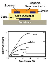
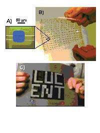
 Figure 1: Schematic of an organic thin film transistor (OTFT).  Figure 2: Electronic Paper, an example of a potent application for flexible, organic electronics. Organic thin film transistors (a) are prepared on a flexible backplane (b) of an electrophoretic display. They allow switching of the pixels of the paper-like display (c). |
Besides the many similarities there are significant differences between these organic and conventional inorganic materials. Weak van der Waals rather than covalent bonds dominate the interaction between the molecules resulting in narrow energy bands for charge transport and in charge carriers that find it more difficult to move from one molecule to another. Nevertheless, at room temperature, mobilities in the range of 1-5cm2/Vs are observed. These are slightly higher than in amorphous silicon but significantly lower than in poly- and single-crystalline silicon where mobilities reach several hundred cm2/Vs. Hence, organic electronics will never be able to compete with silicon CMOS (complementary metal - oxide - semiconductor) technology in terms of speed. So you probably will not expect a computer made of plastic chips any time soon in your near-by computer store.
While silicon chips have superior switching speeds and durability, plastic chips might have the edge on one crucial point: the price. This derives from their ease of handling. They do not require high vacuum equipment. They can be deposited at room temperature from solution, giving hope for low-cost, lightweight, rugged, flexible electronics: plastic electronics. Organic semiconductors should therefore tap a new market, involving applications that demand little from the speed of the circuits, but require that they can be produced in large quantities over large areas and at a low price. Organic, carbon-based materials combine their good semiconducting properties with mechanical properties that permit flexible, lightweight, and distributed electronic and optoelectronic applications ranging from low-end data storage, electronic tags and labels ('electronic barcodes') to smart cards, displays, and toys. Even wearable or disposable computing might be possible. Such low-cost applications represent a formidable challenge for single crystal, polycrystalline, or even low-temperature amorphous silicon technology. Consequently, organic electronics might be able to go where silicon can't follow.
The workhorse of plastic electronics is the so-called organic thin film transistor (OTFT) (see Figure1), which is very similar to the metal oxide semiconductor field-effect transistor-based (MOSFET) silicon technology. The nominally undoped organic semiconductor film is insulating. A negative voltage on the gate electrode attracts electrons to its surface and positive charge carriers (holes) to the interface between the semiconductor and insulator to form an 'accumulation layer'. If a voltage is applied across the source and drain electrodes, a current will flow between them. In this way a small voltage change at the gate electrode can result in a large current change between the source and drain. Consequently, OTFTs can switch and amplify electrical signals as needed for logic operations.
Most of the early organic materials allowed only for p-channel devices, where holes are the major charge carriers, but careful synthetic, organic chemistry and molecular engineering successfully demonstrated n-type transistor materials of similar performance. More recent studies of devices made of high quality single crystals revealed that unintentional dopants and defects were mainly responsible for limiting OTFTs to one type of charge carrier and today several molecular materials have been shown to be capable of p- as well as n channel activity. This could be useful for the development of complementary logic circuits, similar to CMOS technology in silicon devices. The morphology of the organic semiconductor film also has an important impact on the overall device performance, mainly by limiting the charge carrier mobility. However, by optimizing deposition techniques and making use of alignment layers and the self-organizing properties of molecular solids, mobilities in the range of 0.1- 1cm2/Vs have been obtained in various materials. This is already in the right ballpark for the targeted applications but more progress might be expected from advances in materials processing or synthesis of new molecularly engineered materials.
Besides the performance of the semiconductor materials, the right choice of the gate insulator can also play a crucial role for OTFT performance. Both inorganic and organic materials have been used. Organic-based insulators, such as spin-on glass or polyimides, are especially attractive because they are compatible with solution processing on flexible, plastic substrates and their use has led to the demonstration of all-organic transistors.
In order to define the critical device dimension of the OTFT, the channel length or distance between the source and drain electrodes, several low-cost patterning techniques can be used. Some examples are screen-printing, photochemical patterning, microcontact printing, and inkjet printing. These printing techniques are much less sophisticated, and therefore much less expensive, than the optical lithography used in silicon technology. Though the pattern resolution achieved is not as high as with the photolithography employed in fabricating standard CMOS silicon devices, channel lengths of 5mm and even less have been achieved on plastic substrates. As most of these techniques allow reel-to-reel processing, high throughput is possible in production. But their versatility also allows for rapid prototyping and the possibility of customized flexible, electronic circuits.
While transistor performance sufficient for the envisioned applications can be achieved using these low-cost processing and patterning techniques, logic circuits based on individual OTFTs must be prepared in order to commercialize 'plastic electronics'. So far, various companies have demonstrated the integration of a few thousand transistors. In one prototypical application of OTFTs, electronic paper (see Figure 2), plastic electronics are used to drive an electrophoretic display. This was first demonstrated through a collaboration of Bell Laboratories, Lucent Technologies, and E Ink and has now been reproduced by other companies. High voltages and rather low currents are needed to switch the electronic ink pixels, requirements that nicely match the characteristics of the organic transistors. That the display is also only several millimeters thick and bendable reveals the unique capabilities of plastic electronics. With continued progress in materials engineering, processing, and ultra-low cost fabrication techniques, commercial products may become possible and an evaluation of the full potential of plastic electronics would evolve.
The molecular nature of these carbon-based materials offers an intriguing final opportunity - molecular electronics in which logic circuits are based on single molecules or on a single layer of molecules! Recent results on carbon nanotube and self-assembled monolayer-based devices show that transistor action and voltage gain can be achieved in single molecular devices with channel lengths as short as 1 or 2 nm. At these dimensions, the speed of the transistors and number of them per unit area might permit Moore's Law to extend beyond its limits for silicon CMOS technology. Of course, many issues must be addressed before this dream might become a reality. Nevertheless, the future for carbon-based electronics appears very bright indeed!
Hendrik Schön is a Member of Technical Staff in the Nanotechnology Research Department of Bell Laboratories, the research arm of Lucent Technologies. John Rogers is Department Director of the Nanotechnology Research Department. Zhenan Bao is a Distinguished Member of Technical Staff in the Materials Research Department.
©1995 - 2024, AMERICAN PHYSICAL SOCIETY
APS encourages the redistribution of the materials included in this newspaper provided that attribution to the source is noted and the materials are not truncated or changed.
Associate Editor: Jennifer Ouellette
March 2002 (Volume 11, Number 3)
Articles in this Issue

