by P. M. Solomon
Editors Note: This is the first of two articles on advances in electronics. "Plastic Electronics: Going Where Silicon Can't Follow?" by Hendrik Schön, Zhenan Bao, and John Rogers will appear next month.
For the last 40 years, 'Moore's Law' has ruled the growth of the semiconductor industry. This astounding exponential growth of components per chip at a compound rate of 60% per year relies on the product of higher packing densities and larger chip sizes. Higher packing densities have been achieved both by finer lithography as well as by innovations in circuit layout and in self-aligned, device structures. Feature sizes have been reduced by about 100 times during this time, and device count has increased by about 100 million times. For all of this time the silicon metal-oxide-semiconductor field effect transistor (MOSFET) has been the dominant device used in integrated logic and memory chips, and for the past twenty years complementary metal-oxide-semiconductor (CMOS) has been the dominant circuit type.
The power of CMOS lies in its versatility. The CMOS transistor is close to an ideal switch. It draws negligible gate current and can be used in series or in parallel at will. Since complementary switching types are also available, conducting paths can be cut-off in both logic states. Also, the wide band gap of silicon dioxide permits only small tunneling currents even in extremely thin oxide layers, while tunneling is suppressed in the silicon itself by silicon's indirect band gap and relatively large tunneling masses.
Everywhere the trend has been toward replacing other solutions with integrated CMOS, rather than the other way around. For instance, in the early 1990's CMOS replaced the silicon bipolar transistor for most high-end applications even though the bipolar transistor is inherently the faster switching device. III-V technology was developed rapidly in the 1980's to challenge the dominance of silicon in high end switching applications. While III-V technology has secured a niche for itself in the high frequency analog domain, and even in some specialized digital applications, it has never mounted a serious challenge to CMOS. Indeed, competition from III-V technology spurred CMOS toward more aggressive scaling leading to performance levels, integration levels, and low power usage that made it difficult to beat.
CMOS transistors become more leaky as they get smaller due to leakier gate oxides, tunneling leakage in the silicon itself, and thermal leakage over reduced barriers due to reduced gate voltage swings. The latter effect is the major leakage component today, the familiar sub-threshold leakage, but the others become proportionately more important as scaling progresses. In some applications which require very low leakage, the most notably dynamic random access memory (DRAM) and flash electrically erasable programmable read-only memory (EEPROM), device channel length scaling has already effectively stopped, but density continues to increas. High-end servers, where high performance is the primary concern and power is secondary, are at the other end of the applications range. In this environment, scaling can be carried the furthest. So for bulk silicon, scaling can be carried down to ~15 nm for the high performance designs but only to ~25nm for the low power designs. At today's rate of progress and with today's design strategies, this predicament, for the lower power circuits, will be reached before 2014. This does not necessarily mean the end of all progress, since other paths can be explored to continue the performance and density improvements.
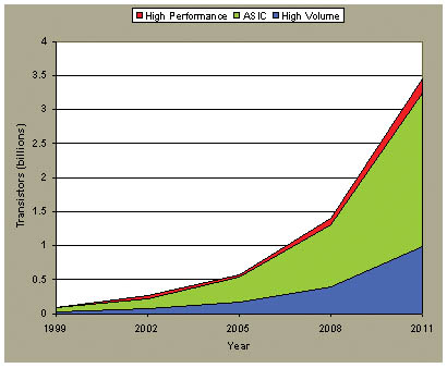
 Figure 1. Number of transistors in each type of chip (400 sq. mm.) as projected from the SIA roadmap. Reprinted with permission from IBM J. Res. Develop. |
Given that CMOS scaling is nearing the end of a long and distinguished journey, why is CMOS still looked upon, almost universally in the industry, as the technology of the future. Instead of ceding applications to other technologies, it is taking over territory. The answer lies in the sheer power of numbers and the ability of 'brute force' scaling to improve performances. Figure 1 shows the numbers of transistors available for different types of applications. It is clear that there is substantial processing power still to be wrung out of CMOS. With billions of transistors potentially available, the question revolves more around how to use them to good effect, given power constraints, rather than finding a way to increase their numbers even more.
Device Design Strategies
As the end of scaling approaches, more radical innovations are being considered, since this may be the only other way to improve performance or to extend scaling a little further. In a sense, today we are in a golden age of semiconductor device research, when radical new device designs, all in CMOS, are needed to exploit the full potential of the technology.
Performance improvements may be gained by improving the transport properties of the silicon itself. There is considerable work today on improving the mobility of silicon by applying strain. The strain induced in the silicon layer caused by accommodating the overlying Si to the larger lattice constant of the SiGe produces a transconductance improvement of about 50%.
The most important factor in scaling is suppressing the tunneling leakage current in the gate insulator. By using a higher dielectric constant material, a thicker insulator may be used for the same degree of charge control. There is much work today in search of alternate dielectrics with a high dielectric constant, yet whose bulk and interfacial electrical properties maintain the standard set by thermal oxide. While this elusive goal has not yet been met, dielectrics such as aluminum oxide and various transition metal oxides show promise.
There is also renewed interest in metal gates. The metal gate eliminates the depletion problem experienced with conventional polysilicon gates and, with suitable work function, may give improved channel mobilities by reducing channel doping. Another possible benefit is circumventing the mobility reduction that is predicted to occur in very thin oxides due to remote interactions between electrons in the channel and plasmons in the polysilicon gate. The search for a suitable work function, combined with low reactivity toward the gate dielectric, has led toward pure metals like tungsten as well as metallic compounds such as transition metal nitrides and silicides.
Improvements in scaling are predicted to occur for thin silicon-on-insulator (SOI) films, with thickness of order of 10nm or less. The thickness limit is probably about 3nm because quantum effects make the band gap (and hence threshold voltage and channel potential) very sensitive to thickness, so that slight fluctuations in thickness cause large fluctuations in potential. Experiments have thus far confirmed adequate mobilities down to ~5nm thickness, opening a 5-10nm window for thin SOI devices. Although the configuration of a single-gate FET (SGFET) in SOI is attractive, because of its simplicity and because excellent device results have been shown by IBM and Intel at gate lengths of 33 and 50nm, the easy penetration of electric field beneath the FET when the SOI is fully depleted severely limits its scaling potential. Better scaling is obtained with a double-gate FET (DGFET) in which there is a gate on both sides of a thin silicon layer. Then, when using the higher dielectric constant insulators, mentioned earlier, the reduction in scaling length might approach a factor of two. The two gates of the DGFET augment this advantage since they may be controlled independently, offering advantages of extra functionality.
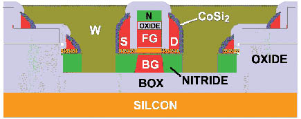
Research into DGFETs has picked up pace in universities such as Berkeley and MIT, and in the industry such as at IBM and Lucent. Fig. 2 shows a cross-section of an experimental self-aligned planar DGFET, realized at IBM, where the source and drain regions are etched away to leave sidewalls and to allow the back gate to be under-cut.
 Figure 2. Schematic cross-section of an experimental planar DGFET structure, by an IBM group, showing silicided sidewall self-aligned S/D, tungsten self-aligned S/D plugs, and isolated undercut back gate |
Power Management.
Of all the issues that confront scaled integrated circuits, power dissipation is the most serious. Though the power per function continues to decrease, more and more functions are crammed onto ever larger and denser chips. There is also an increasing conflict between the demands for low dynamic power, which requires low power supply voltages, and low standby power that needs higher threshold voltages to turn the transistors off. This trade-off leads to power supply optimization and device design according to application.
Power management technology is still in its early stages of development, since until recently voltage reduction, improvements in cooling technology, and improvements in system architecture have kept the problem within bounds. But within the domain of device design, several approaches could result in a better static versus dynamic power trade-off, such as multiple threshold voltages; multiple oxide thicknesses and power supplies; dynamically adjustable threshold voltages and block switching.
Of these, block switching, in which the power supply to a circuit block or even an entire processor is gated, is the more radical approach. If the gating switch consists of a high threshold voltage, thick gate oxide FET, both the sub-threshold and gate leakage components of the standby power may be greatly reduced. At issue are the size, speed and power needed to switch the switching transistor but detailed analysis shows its practicality and the plausibility of its increased use in future chip-systems.
Redundancy
A premise of many of the power management schemes is that devices are cheap but power is expensive in future chip-systems. At issue is whether devices are used to implement large numbers of
processors on a chip, many of them idle because of power constraints, or whether the transistors are better used with fewer processors and a very large cache memory. Most likely a particular balance will be struck depending on the application, but the availability of 10 billion transistors in `end of road-map' chips allows for placement of hundreds of processors, and innovations like embedded DRAM (or other dense on-chip memory technology), might mean that there is adequate chip area to support large numbers of processors, each accompanied by a large cache.
Redundancy is now an essential part of memory design, including error detection and correction. Without it memory could never achieve the integration levels available today. It is not an unwarranted speculation to assume that it will be equally important for future chip-systems. The increased susceptibility of scaled devices and circuits to soft errors, increasing parameter spreads caused by material fluctuations, and increasing numbers of devices point to the need for such techniques, while the increased on-chip computing power gives an increased capability of implementing them. Redundancy techniques have long been applied to fault tolerant and highly reliable computing systems and have been implemented in hardware and software and at high and low levels. This is an important area for research and a possible key for exploiting future systems to the full.
The data processing potential of future CMOS chips is tremendous. Even as we push up against ultimate limits, device designers will exploit structural possibilities to the utmost, continuing density and performance improvements for many generations to come. Indeed, the ultimate MOSFET is truly a 'nano-transistor', competitive with other nano-challengers. A device scaling approaches its logical conclusion, the future of the VLSI revolution will be even more in the hands of the chip architect.
Paul Michael Solomon is a research staff member at the IBM T.J. Watson Research Center, Yorktown Heights, NY.
©1995 - 2024, AMERICAN PHYSICAL SOCIETY
APS encourages the redistribution of the materials included in this newspaper provided that attribution to the source is noted and the materials are not truncated or changed.
Associate Editor: Jennifer Ouellette
February 2002 (Volume 11, Number 2)
Articles in this Issue

