By Calla Cofield

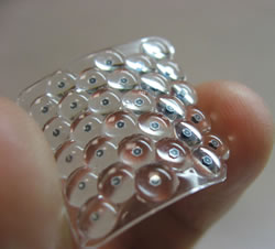
A flexible mechanical model with embedded microscale photovoltaic cells.
Solar cells on the market today are most often made of crystalline silicon, used because of its high light-to-energy efficiency. Silicon is also the primary material used in semiconductors and computer electronics, which have seen a rapid decrease in cost over the past three decades. So, “Why shouldn’t the solar industry see a similar drop in price?” says Vipin Gupta, a co-lead in Sandia’s Microsystems Enabled Photovoltaics group. “There seems to be an intuitive sense that the two ought to be connected.”
At a press conference at the APS April Meeting, Jeff Nelson held up the product of Sandia’s efforts to combine these two fields: a vial of liquid containing solar cells so small they look like bits of decorative glitter, which has earned them the nickname “solar glitter.”
Basic crystalline silicon solar cells are made from wafers of silicon roughly four to six inches squared and 200 microns thick. Each wafer makes a single cell, and the cells are lined up together to make solar panels that must be placed between plates of glass for handling. Overall this makes the panels rigid and heavy. The Sandia team has managed to cut up the solar silicon wafers into many smaller cells, between 100 and 750 microns squared, and thin them down to 10 to 20 microns thick.
Individual cells cut from the same piece of silicon can be connected into single panels, but mounted in flexible, light-weight materials rather than glass. Eventually, this could mean solar cells in fabric, such as clothing or tents, and solar panels that fit a wide variety of surfaces and are easily relocated.
Other thin-film solar cells exist on the market, but Nelson says these films don’t use crystalline silicon, which reduces their efficiency. To create solar glitter, Nelson says the Sandia team used “standard layer transfer techniques”: a sticky polymer film with an interconnect pattern is applied to the top of the 200 micron thick wafer, and then pulled away, taking an array of new, 10 to 20 micron-thick solar cells with it. More than 90 percent of the light conversion takes place in the first 20 microns of a solar cell, so little efficiency is lost. After pulling off the top layer of the silicon wafer, the remaining silicon can be used to create more cells, cutting down on the cost of the material and leaving none to waste.
“Other folks have been able to take a wafer and release small layers, but it takes a long time, and that drives up the cost and is not manufacturable,” said Nelson at a press conference at the April Meeting. Those processes also take much longer than the peel-off method used by Sandia, which Nelson says allows the scientists to “release those cells when we need them.”
Using smaller cells means that many techniques and tools from the semiconductor and microelectronics industry are available to solar panel engineers. The solar glitter cells are more robust than larger cells, so they can be handled with so-called “pick ‘n’ place” tools that handle microelectronics, which means more of the production processes are already established. Gupta says the smaller cells also allow for different “interconnect architectures,” which the team is already using to give the cells better performance in partial shade–the efficiency of most solar cells goes down when they are not exposed to full sunlight. And the team is working on incorporating a device called a “micro-concentrator,” which focuses more light into each individual cell, increasing its total absorption, and lowering the cost per watt.
The Sandia scientists are also using techniques from integrated circuit science to bond three types of solar glitter together–one made of silicon, one made of gallium arsenide, and one made of indium gallium phosphide–rather than using the more expensive process of growing them together. Collectively the different materials gather more wavelengths of light, and increase the cell’s efficiency.
“What we’re providing is the specific way to do design, simulation, fabrication, assembly, packaging and characterization of [solar] cells using semiconductor, LCD and microsystem tools,” said Gupta. “We’re laying out, here’s how you do it, step by step.”
Over the next two to three years Nelson says the project will continue within Sandia, where he says “we will take a lot of the concepts and cells we’ve produced and develop them into larger applications.” After that, the lab intends to find partners in industry to commercialize the technology.
©1995 - 2024, AMERICAN PHYSICAL SOCIETY
APS encourages the redistribution of the materials included in this newspaper provided that attribution to the source is noted and the materials are not truncated or changed.
Editor: Alan Chodos
June 2012 (Volume 21, Number 6)
Articles in this Issue

