September 1981: Invention of the scanning tunneling microscope
  |
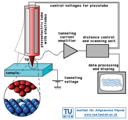
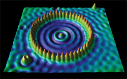
Classically, electron flow is not possible without a direct connection, such as a wire connecting the two surfaces. However, on the atomic scale, when the distance between two surfaces is small enough, there is a finite probability that an electron will jump from one surface to another of lower potential In the case of the STM, the tunneling current starts to flow when a sharp tip approaches a conducting surface at a distance of approximately one nanometer. The tip is mounted on a piezoelectric tube, which undergoes tiny movements when a voltage is applied to its electrodes. The tip position is controlled by the electronics so that the tunneling current, and hence the tip-to-surface distance, is kept constant as it scans a sample surface. This movement is recorded and can be displayed as an image of the surface topography. Recording the vertical movement of the stylus makes it possible to study the structure of a surface atom by atom.
When the first conventional optical microscope was invented, it represented a tremendous achievement for scientific research, particularly in biology and medicine. However, as the technology continued to improve, scientists discovered that there were fundamental limits to optical techniques because of the wave characteristics of light. Using light waves, it is impossible to distinguish details smaller than the wavelength of the light. Another significant breakthrough in microscopy occurred when it became possible to produce an image of an object using an electron beam, recorded on a fluorescent screen or a photographic plate. Scientists were even able to increase the magnification by combining two or more lenses. Ernest Ruska, a scientist with the Max Planck Institute in Berlin, made the most important fundamental contributions to electron optics and designed the first electron microscope.
In Ruska's design, called the transmission microscope, the object to be examined is in the form of a thin section. The electron beam pierces the object in much the same way as light does in a conventional microscope. Then came the complementary scanning electron microscope, in which a sharply focused electron beam strikes the object. The principle behind the STM is quite different. A mechanical device is used to sense the structure of a surface, similar to how the reader's fingers detect the impressed characters in Braille. It is possible to obtain a much more detailed picture of the topography of a surface if it is transversed by a fine stylus whose vertical movement is recorded. The sharpness of the stylus determines the resolution. Because small structural details of the surface can be damaged by mechanical contact, it is necessary to maintain the stylus at a small, constant distance from the surface.
The first researchers to succeed in building an STM were Gerd Binnig and Heinrich Rohrer at IBM Research Laboratories in Zurich, Switzerland, largely because of the exceptional precision of their mechanical design. They eliminated environmental vibrations by building the microscope upon a heavy, free-floating magnet in a dish of superconducting lead. Later on, less bulky but equally effective devices for stable, disturbance-free suspension of the microscope were developed, using piezoelectric elements to control the horizontal movement of the stylus. The vertical movement of the stylus is controlled and measured using another piezoelement. And it is now possible to produce styluses whose tip consists of a single atom, giving unprecedented resolution and the ability to depict individual atoms to study the atomic structure of the surface being examined.
The two scientists submitted their first paper on their invention of the STM in September 1981 to Applied Physics Letters. And in 1986, Binnig and Rohrer shared the Nobel Prize for physics (with Ruska) for their work on the STM. Thanks to their achievement, entirely new fields have opened up for studying the structure of matter, particularly in surface physics, which has important applications in semiconductor physics and microelectronics. Another major area of current STM research is the study of self-assembled monolayers (SAMs), a single layer of molecules which aggregates on a surface. In other sciences, surface chemistry plays an important part in catalysis, and it is also possible to fixate organic molecules on a surface and study their structure, a technique that has been used to study DNA molecules.
©1995 - 2024, AMERICAN PHYSICAL SOCIETY
APS encourages the redistribution of the materials included in this newspaper provided that attribution to the source is noted and the materials are not truncated or changed.
Associate Editor: Jennifer Ouellette
August/September 2003 (Volume 12, Number 8)
Articles in this Issue

